Your circuit is designed and ready to go. Testing and modeling have shown that it works beautifully. Now, the next step is to create a printed circuit board based on your design to bring your project to life. Whether it’s a school or college project, or the final piece of an electronic device produced by your company, implementing the circuit on a printed circuit board looks professional and provides a much clearer idea of the final product.
Printing the PCB
Step 1. Choose a method for creating the printed circuit board.
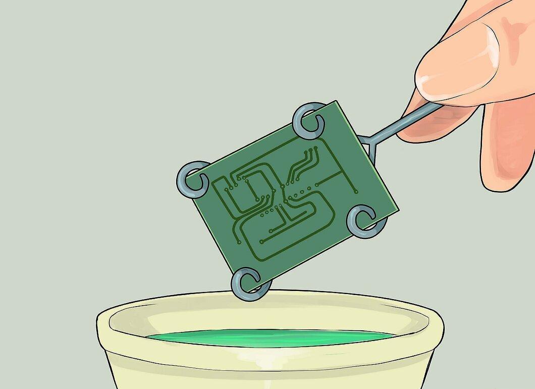
Choose a method for creating the printed circuit board. The method usually depends on the available materials and the complexity and quality of the PCB required. Below is a brief description of various methods and their distinct features.
Step 2. Create the layout of the printed circuit board.
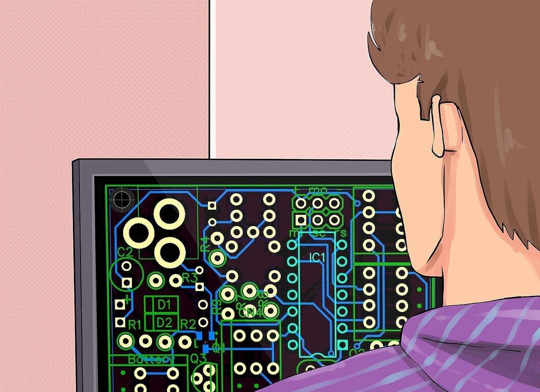
Create the layout of the printed circuit board. For the chemical etching method, you need to draw the board using a material that does not react with the etchant. If you want to draw it by hand (not suitable for precise and complex circuits), specialized markers are available for this purpose. However, the most common tool is ink for laser printers. Typically, the PCB layout is printed based on its schematic using specialized software. There are many free computer programs available for designing and creating PCB layouts. Here are some websites where you can find such software (in English):
- Liquid PCB
- ShortCut
Step 3. Once you create the PCB layout on your computer, adjust its size using the appropriate software to match the PCB blank.
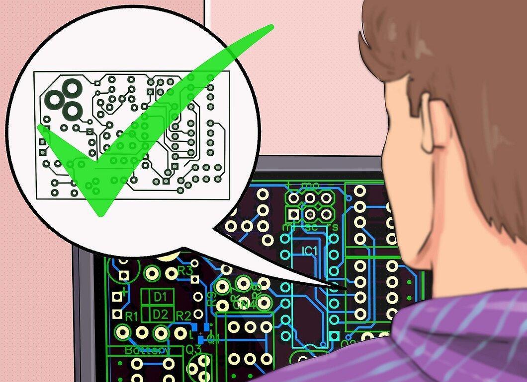
Step 4. Print the layout from the “File” menu.
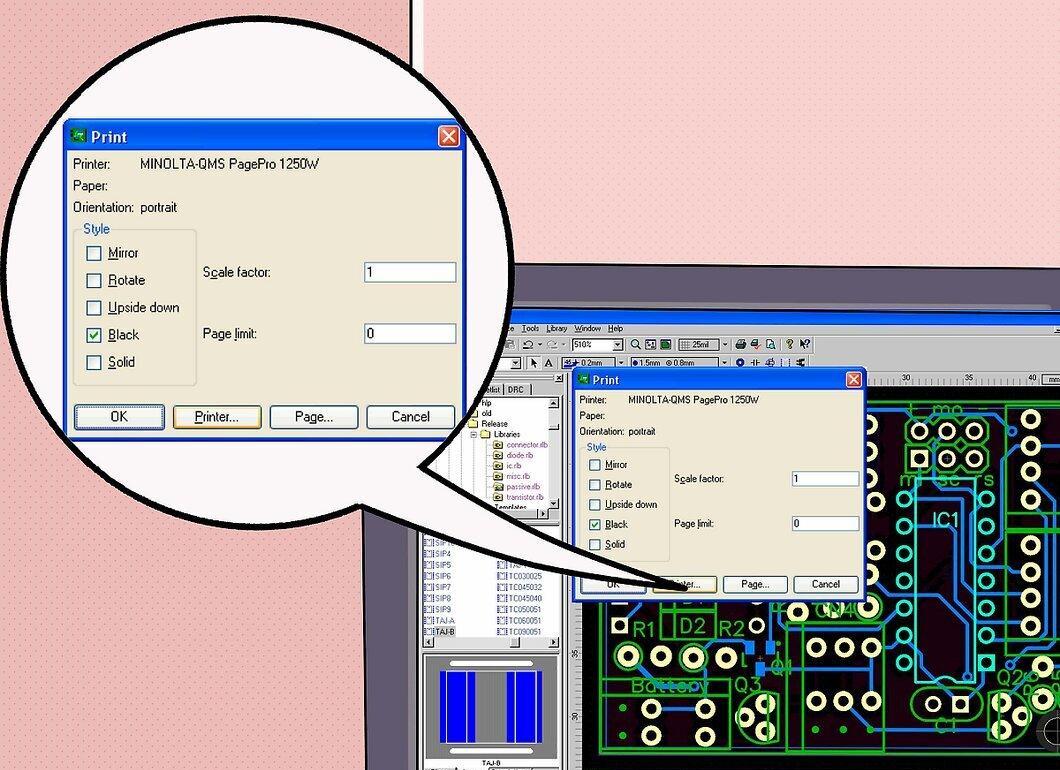
Print the layout from the “File” menu. Print the layout on glossy paper, such as magazine paper. Before printing, make sure that the layout is mirrored (most PCB design software offers this option when printing). After that, avoid touching the side of the paper where the PCB layout is printed.
Step 5. Place the printed paper on the PCB blank (with the layout facing the copper coating of the blank).
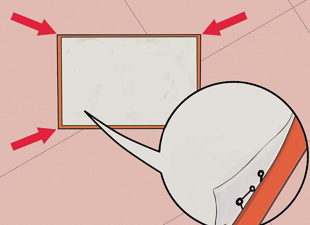
Place the printed paper on the PCB blank (with the layout facing the copper coating of the blank). Turn on the iron. Set the iron to the silk setting and wait for it to heat up.
Step 6. When the iron is heated, carefully place it on the paper with the layout on top of the PCB blank.
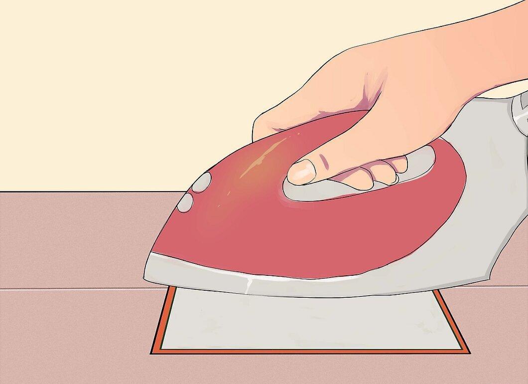
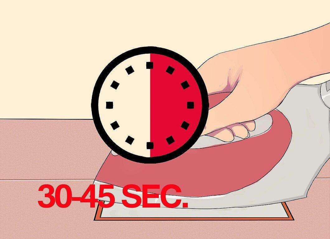
Step 7. Hold the iron on the paper for 30–45 seconds (depending on the brand of the iron).
Step 8. After removing the iron, carefully set it aside, take the PCB blank, and bring it to the nearest water source.
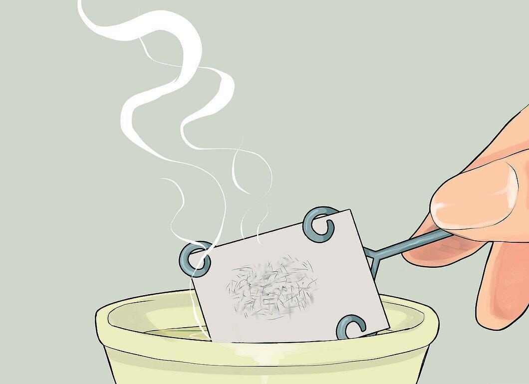
After removing the iron, carefully set it aside, take the PCB blank, and bring it to the nearest water source. Be cautious, as the paper will be hot. The paper should adhere to the blank, so ensure it doesn’t tear off.
Step 9. Turn on the tap and hold the blank with the paper under the stream of water.
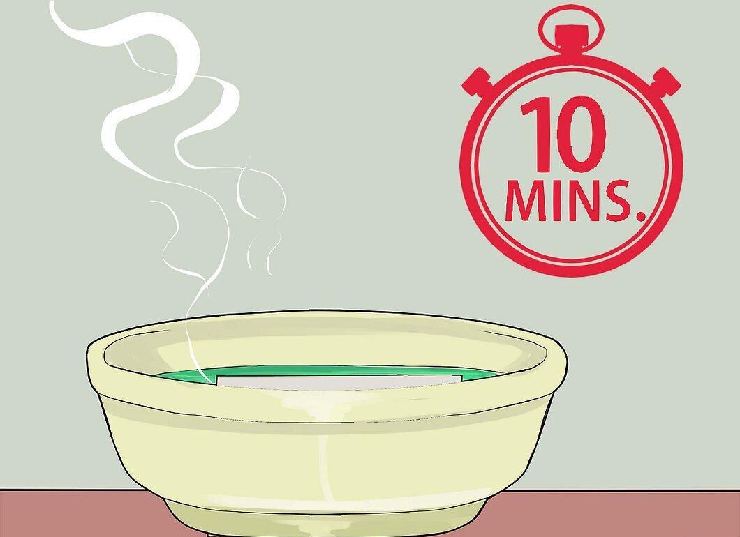
Turn on the tap and hold the blank with the paper under the stream of water. You can also submerge the blank with the paper in hot water for a few minutes, but not more than 10 minutes.
Step 10. Gently peel the paper off the blank.
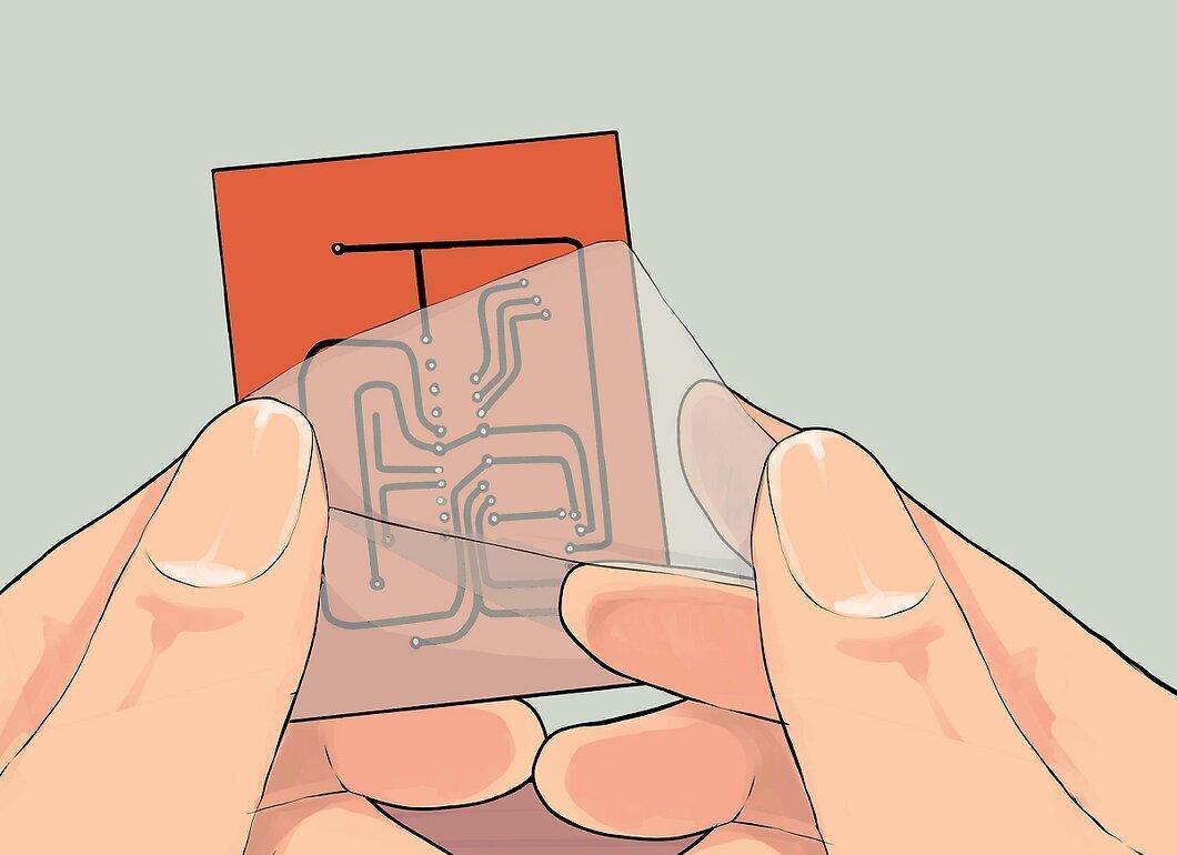
Gently peel the paper off the blank. If it’s difficult to remove the paper in some areas, try wetting it again. You should end up with a copper surface of the blank with traces of black printer ink on it.
Step 11. Dry the blank.
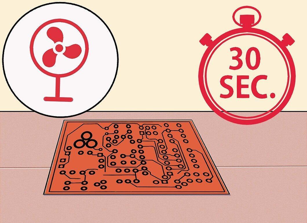
Dry the blank. Gently remove large water droplets with a soft napkin or sponge, or simply shake the board. Be careful and aim to do this within 30 seconds; otherwise, the ink may come off.
Step 12. Etch the PCB using one of the methods described below.
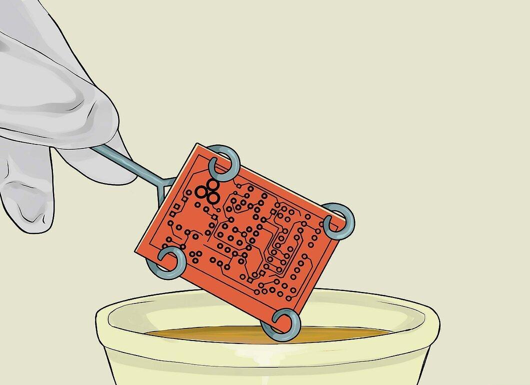
Etch the PCB using one of the methods described below. This way, you will remove the copper where it is not needed, leaving conductive traces where the ink remains.
Chemical Etching
Step 1. Choose an etching acid.
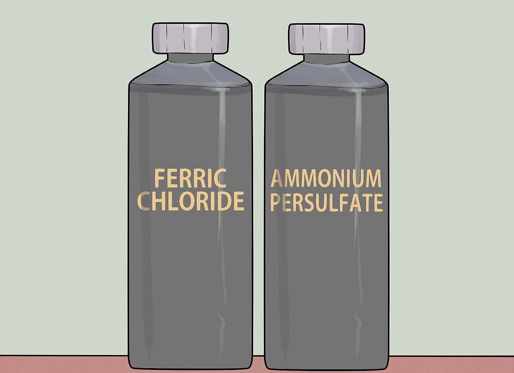
Choose an etching acid. Ferric chloride is commonly used as an etchant for PCBs. Ammonium persulfate or other chemical solutions can also be used. Regardless of which chemical you choose, remember that it is a highly dangerous material, so follow not only the safety measures described in this article but also carefully read the instructions for the substance you choose.
Step 2. Prepare the etching solution.
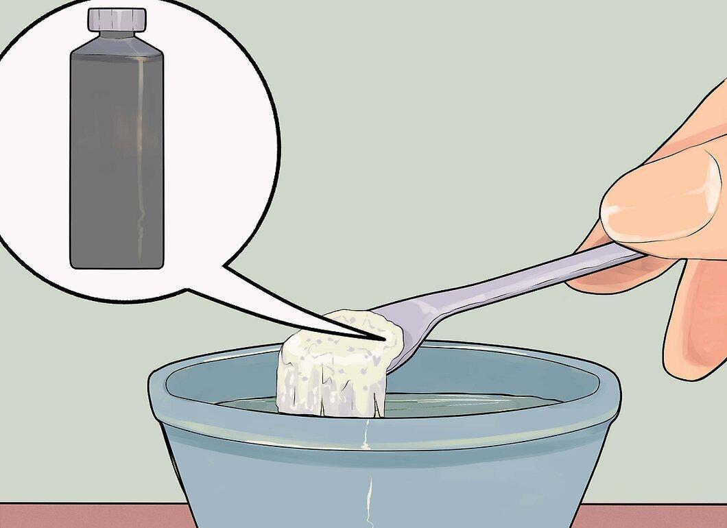
Prepare the etching solution. Depending on the acid chosen, additional steps may be required. For example, crystallized acid should be dissolved in hot water, while other etchants may be ready to use.
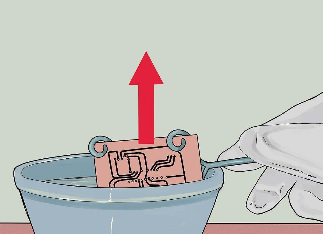
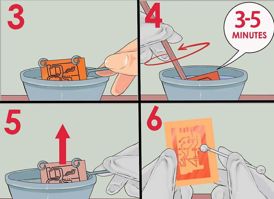
Step 3. Immerse the PCB blank in the acid.
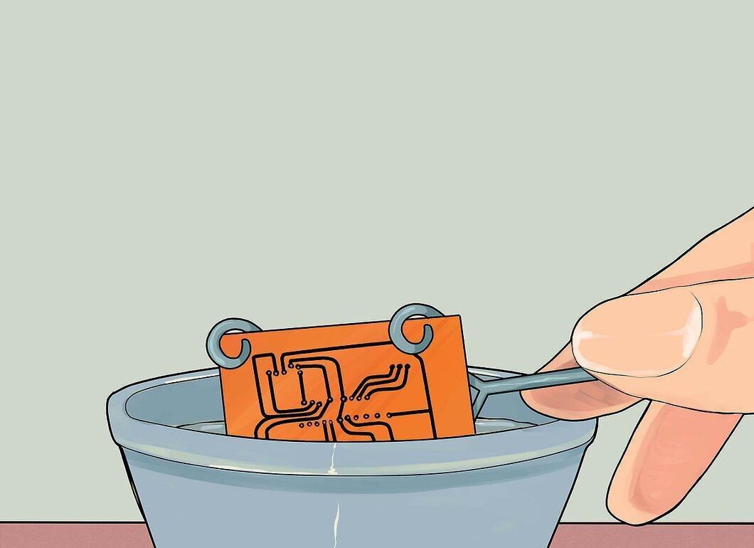
Step 4. Flip the board every 3–5 minutes.
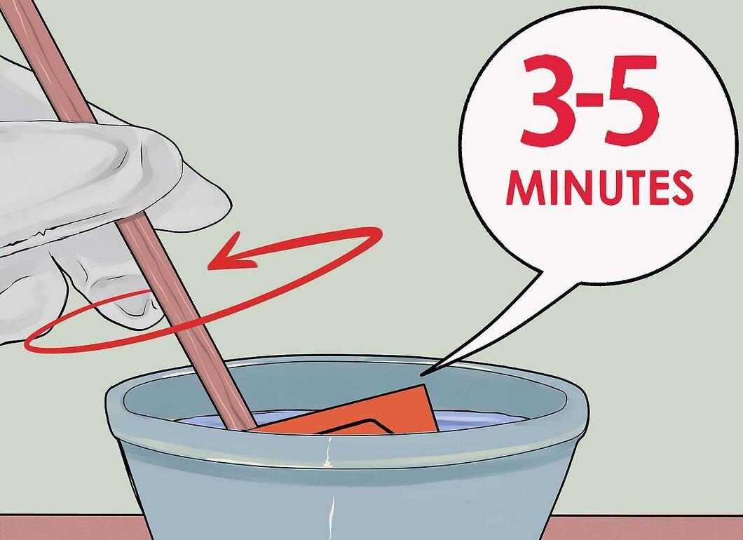
Step 5. Remove the board and wash it after all excess copper has been etched away.
Step 6. Clean the board from the substance covering the conductive coating.
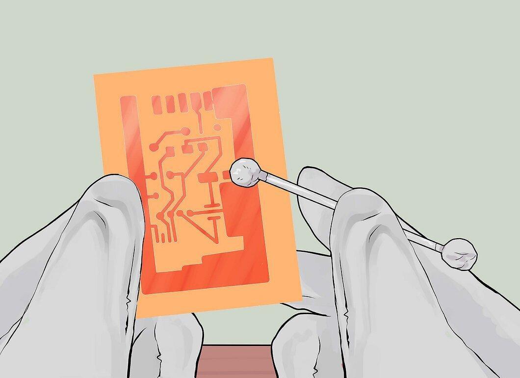
Clean the board from the substance covering the conductive coating. There are many specialized solvents for this kind of material used in PCB manufacturing. If you cannot use specialized means, fine-grit sandpaper can be used.
UV Exposure Method
Step 1. For this method, you will need a blank covered with photosensitive film (for positives or negatives), a UV etching device, a transparent sheet, and distilled water.
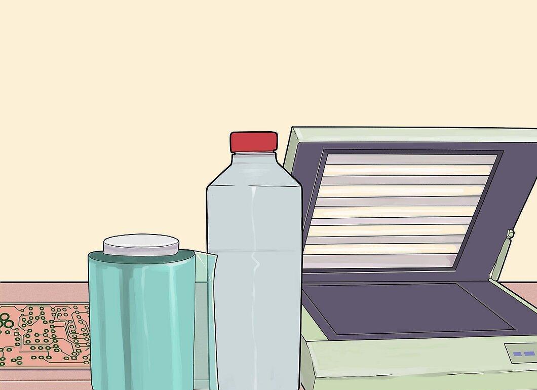
For this method, you will need a blank covered with photosensitive film (for positives or negatives), a UV etching device, a transparent sheet, and distilled water. You can purchase suitable blanks (they are covered with black nylon film), or apply a photosensitive spray to the copper-coated side of a regular clean blank. Additionally, don’t forget to buy the developer for the corresponding spray or photosensitive coating.
Step 2. Use a laser printer to print the PCB layout on the transparent sheet in positive or negative format, depending on the type of photosensitive coating on the board.
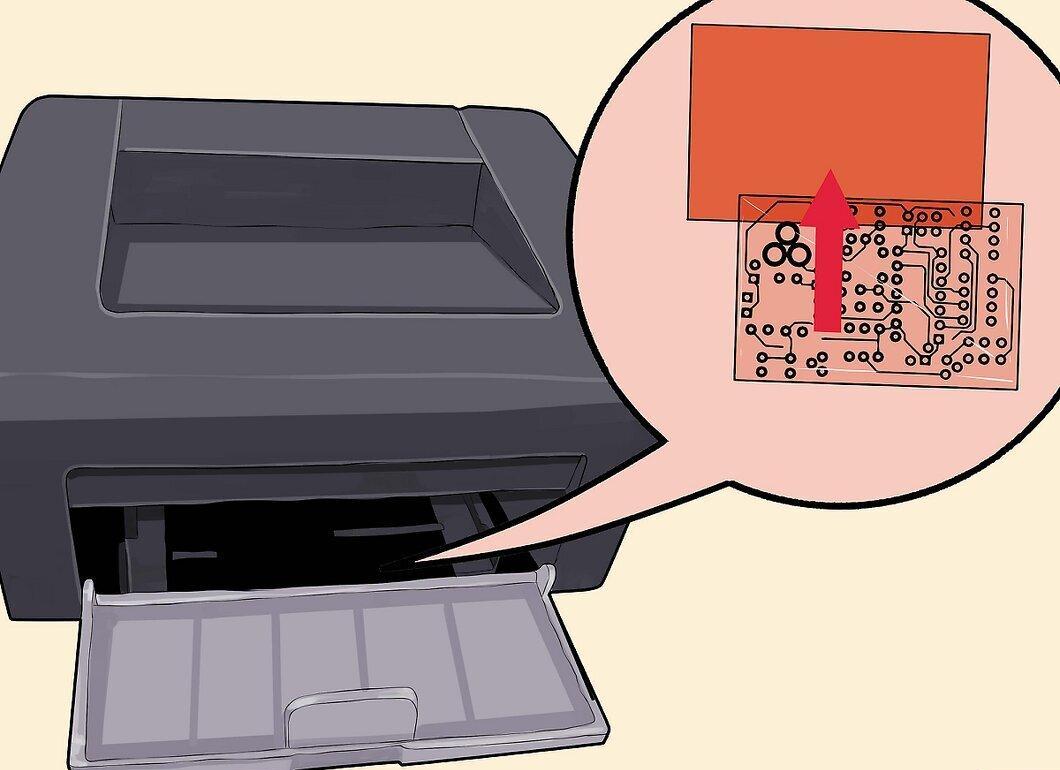
Step 3. Place the transparent sheet with the printed layout on the copper-coated side of the board.
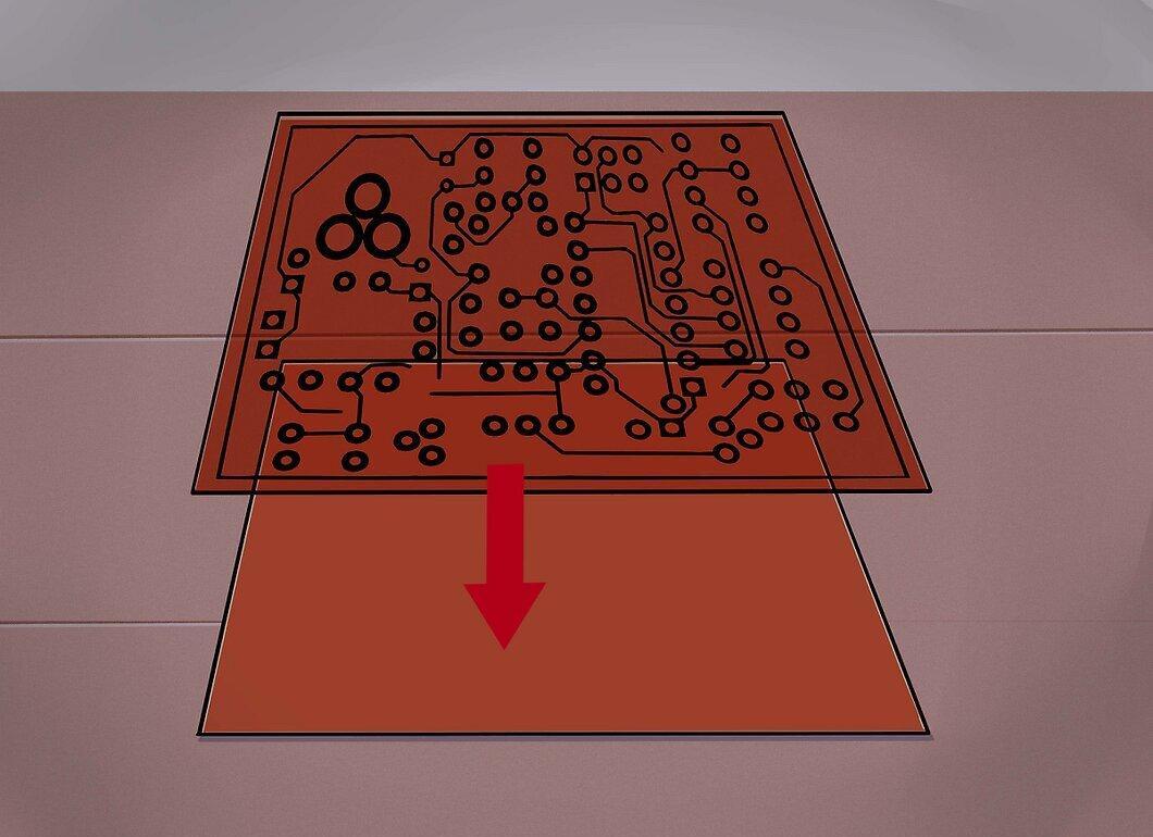
Step 4. Place the board in the UV etching device.
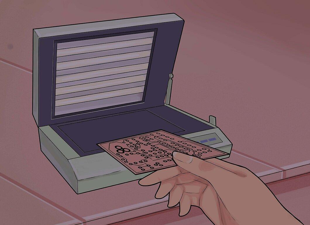
Step 5. Turn on the UV etching device.
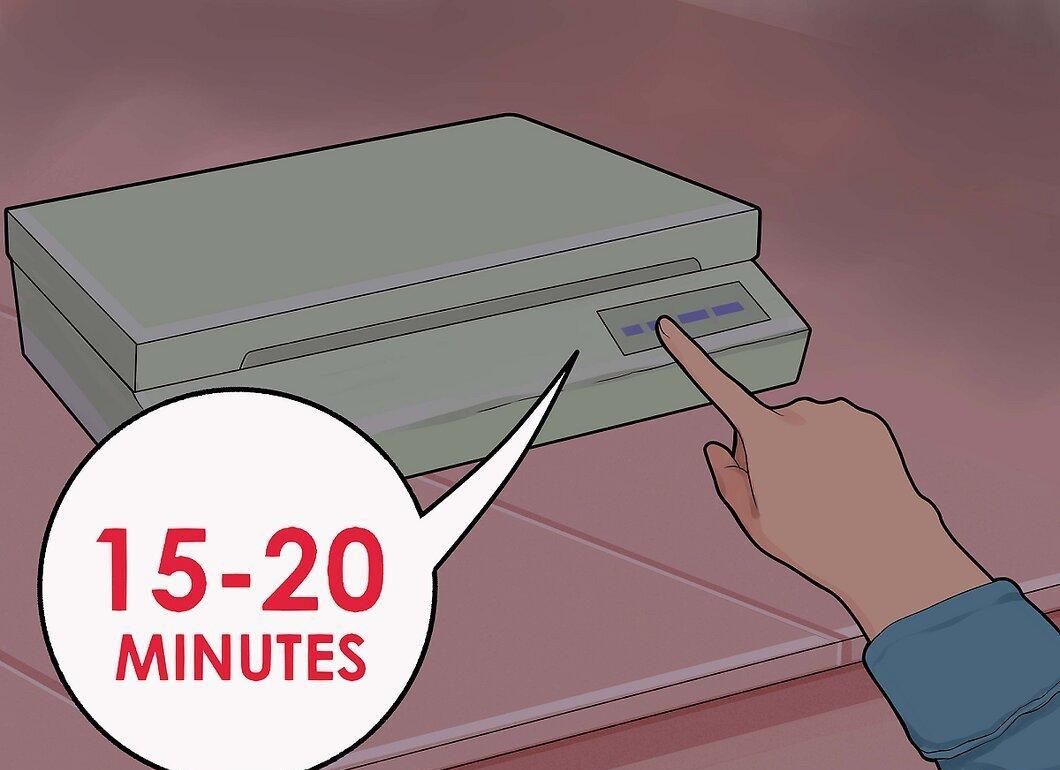
Turn on the UV etching device. As a result, during the set time, the board will be exposed to ultraviolet radiation. Most UV etching devices are equipped with a timer. Generally, 15–20 minutes is sufficient.
Step 6. After that, remove the board from the device.
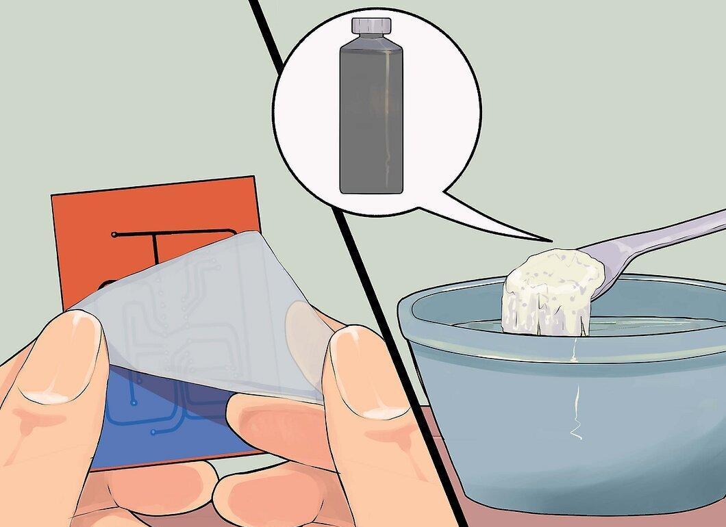
After that, remove the board from the device. Apply the developer to the copper-coated side and gently rinse it with distilled water before placing the board in the acid bath. The acid will etch the areas that reacted with the ultraviolet radiation.
Step 7. Further steps are described in the chemical etching section (steps 3–7).
Completing the PCB
Step 1. Drill holes for mounting points.
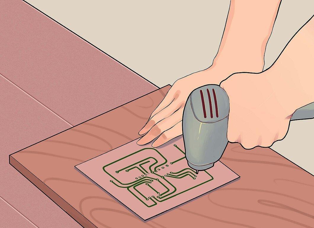
Drill holes for mounting points. Typically, specialized drilling machines are used for this procedure. However, a regular drill can be adapted for this task in home settings.
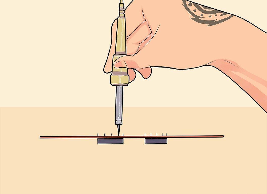
Step 2. Secure the finished PCB and solder the electronic components to it.